An Introduction to Semiconductor Wafer
The semiconductor technology is quite complex and critical in nature. There are a number of processes, equipment’s and sub systems needed to complete semiconductor manufacturing process. Semiconductors are found in almost all electronic devices hence they are significant in nature. From handling the raw silica to producing the semiconductor, a number of processes and techniques are involved. Various components of semiconductors have its own manufacturing processes. One such component is semiconductor wafer.
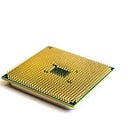
What is Wafer?
Wafer is a thin slice of semiconductor, mostly made up of silicon which used in fabrication of integrated circuit. This silicon wafers are a key component in the production of the semiconductors. Wafer itself goes through its fabrication process so that the quality and performance remain high, and the wafers works efficiently.

Wafer Production:
A wafer is first produced from the silicon. In this process, purified polycrystalline silicon is heated to a molten liquid. A small piece of solid silicon is placed on the molten liquid. As the silicon is slowly pulled from the melt, the liquid cools to form a single crystal ingot. The wafer is then processed through a series of machines, where it is ground smooth and chemically polished to a mirror-like lustre.
Wafer Fabrication Process:
Once the wafer is produced it is fabricated afterwards to get the best results. The fabrication process, which takes place in a clean room, involves a series of steps and the process can take anywhere from 10 to 30 days to complete. In Silicon wafer fabrication process a number of steps are involved such as Grinding, Slicing, Rounding, Lapping, Polishing, Cleaning, Inspection, Packing and Shipping.
Wafer Fabrication Equipment:
Various wafer fabrication equipment are used to produce and improve the wafer fabrication process. The main objective of wafer fabrication equipment is to remove, grow or deposit material on the wafer. Oxidation system, epitaxial reactors, diffusion systems, ion implantation equipment, physical vapor deposition systems, chemical vapor deposition systems, photolithography equipment, and etching equipment are examples of wafer fabrication equipment’s.
The demand for such equipment’s is increasing exponentially as the demand for advanced and improved semiconductor wafers is increasing. The wafer fabrication market has shown tremendous growth in recent times. Global wafer fabrication equipment market is projected to witness a CAGR of 3.07% during the forecast period to reach a total market size of US$61.886 billion by 2023, increasing from US$51.618 billion in 2017.
Conclusion:
Wafer fabrication process is a complex process which involves a number of advanced mechanisms techniques. Due to the involvement of high criticality and risk if the process is not executed properly, only a handful of companies carries out wafer manufacturing and fabrication process. Elkem, MEMC Electronic Materials, Mitsubishi / Sumitomo Sumco Silicon (Sumitomo Metal Industries) are some of the biggest manufacturers of semiconductor wafers.